India Semiconductor Mission: All you need to know about Centre’s bold leap to become global microchip hub

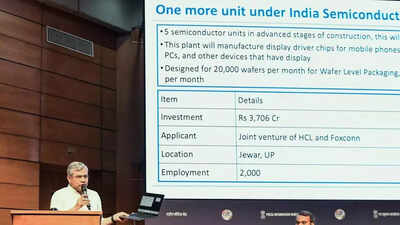
NEW DELHI: The Cabinet on Wednesday approved a new semiconductor plant in Jewar, Uttar Pradesh. The plant, to be set up by the HCL-Foxconn joint venture, will produce display driver chips for mobile phones, laptops, and cars under the “India Semiconductor Mission.”“The Cabinet has approved a sixth semiconductor plant. It is a joint venture between HCL and Foxconn to manufacture display driver chips. These chips control the quality and format of the content displayed on screen. It is a very advanced technology that is being set up,” Information and broadcasting minister Ashwini Vaishnaw said while briefing the media on the Cabinet decision.“What we understand is that once this unit is there, then the display panel plant will also come to India. This will meet 40 per cent of India’s capacity. It is a large plant. It will also meet the requirements of Foxconn for the rest of the world,” he added.
All you need to know about the Semiconductor plant
Sixth Semiconductor unit: The newly approved plant is a joint venture between Indian tech giant HCL and global electronics manufacturer Foxconn. It will be located near Jewar Airport in the Yamuna Expressway Industrial Development Authority (YEIDA) region of Uttar Pradesh.Investment of Rs 3,700 crore: With an investment of Rs 3,700 crore, this new plant will attract significant domestic and foreign investment, strengthening India’s industrial base and creating high-tech jobs.Focus on display driver chips: The facility will specialise in manufacturing display driver chips, which are essential for devices like mobile phones, laptops, PCs, cars, and other consumer electronics with displays. The upcoming plant will produce display driver chips — essential components that control how content appears on screens and other electronics.
- It will have the capacity to handle 20,000 wafers per month.
- The output will be around 3.6 crore (36 million) chips per month.
- These chips manage the function and format of visuals on digital displays, making them crucial for everyday gadgets.
Growing semiconductor ecosystem: India now has five semiconductor units already in advanced construction, with this sixth marking another critical milestone. Global players like Applied Materials and Lam Research (equipment), and Merck, Linde, Air Liquide, and Inox (gas and chemical suppliers), have already set up or are expanding operations in India to support this ecosystem.R&D and design push: Students and entrepreneurs from 270 academic institutions and 70 startups are working on cutting-edge design technologies to develop new products. 20 products created by students have been taped out by SCL Mohali.
What is India Semiconductor Mission (ISM)
The India Semiconductor Mission aims to make India a global hub for electronics manufacturing and design by building a strong and innovative semiconductor and display ecosystem.Vision: To create a vibrant and advanced environment for semiconductor and display design, encouraging innovation and helping India become a global leader in electronics manufacturing.Strategy: ISM focuses on creating a long-term plan to develop semiconductor and display manufacturing facilities and a strong design ecosystem.Design & Startups: ISM supports the growth of the Indian semiconductor design industry by helping early-stage startups. It provides tools like Electronic Design Automation (EDA), access to chip manufacturing services (foundries), and other resources needed to innovate and grow.Supply Chain: ISM also works to build a secure and reliable supply chain for electronics. This includes ensuring the availability of key raw materials, specialty chemicals, gases, and advanced manufacturing equipment needed to produce semiconductors and displays.This initiative is central to India’s broader mission of “Atmanirbhar Bharat”, ensuring the country can meet growing demand for semiconductors driven by expansion in electronics, defence, healthcare, and AI sectors.


